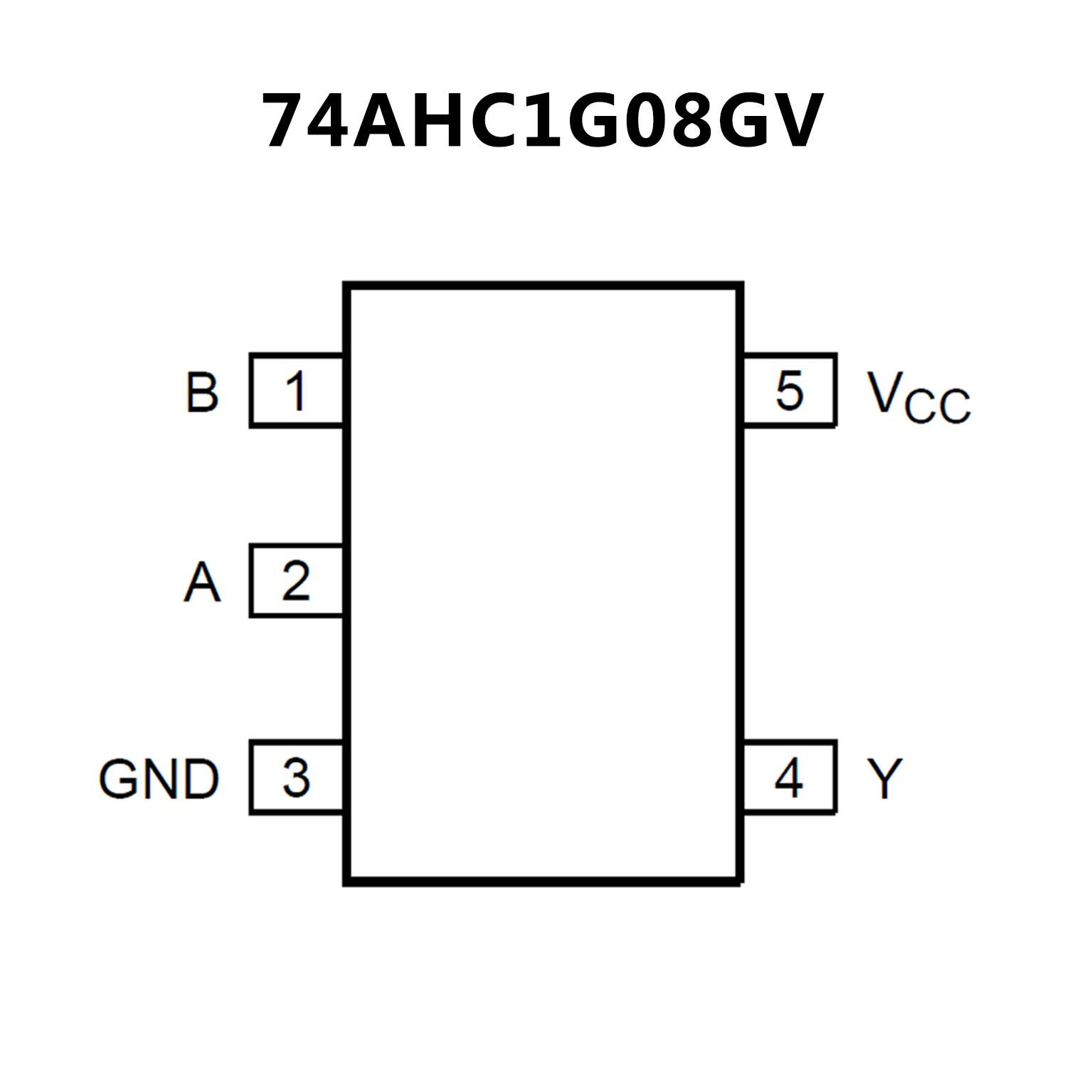
 74AHC1G08.pdf
• Wide Supply Voltage Range: 2.0V to 5.5V
• +8mA/-8mA Output Current at VCC = 5.0V
• Low Quiescent Current: ICC = 2μA (MAX)
• Propagation Delay:
tPD = 4.5ns (TYP) at VCC = 5V and CL = 50pF
• All Inputs with Schmitt-Trigger Action
• -40℃ to +125℃ Operating Temperature Range
• Available in Green SC70-5 and SOT-23-5 Packages
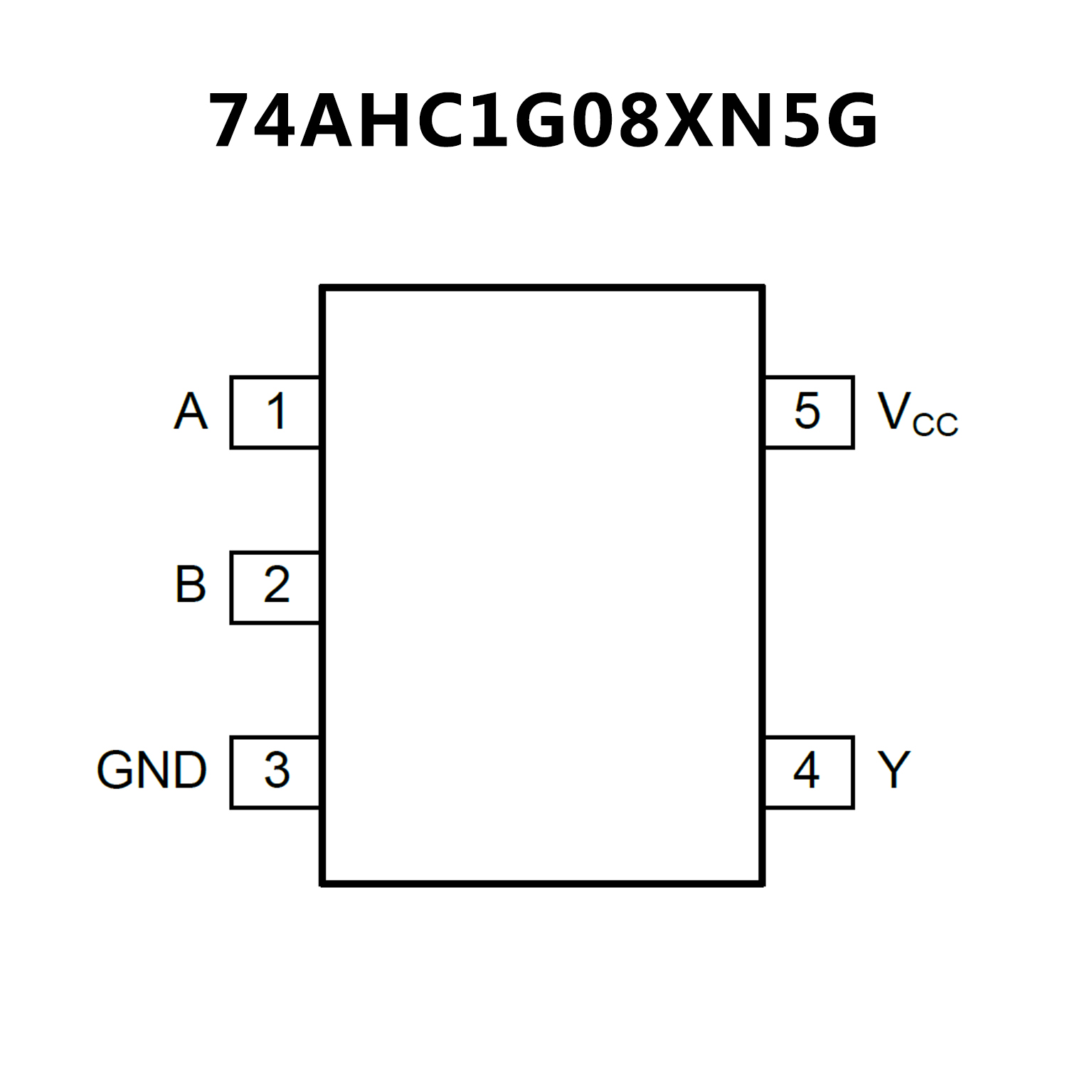
• Wide supply voltage range from 2.0 to 5.5 V
• Overvoltage tolerant inputs to 5.5 V
• High noise immunity
• CMOS low power dissipation
• Latch-up performance exceeds
100 mA per JESD 78 Class II Level A
• Symmetrical output impedance
• Balanced propagation delays
• Input levels:
• For 74AHC1G08: CMOS level
• For 74AHCT1G08: TTL level
• ESD protection:
• HBM JESD22-A114E: exceeds 2000 V
• MM JESD22-A115-A: exceeds 200 V
• CDM JESD22-C101C: exceeds 1000 V
• Specified from -40 °C to +125 °C
