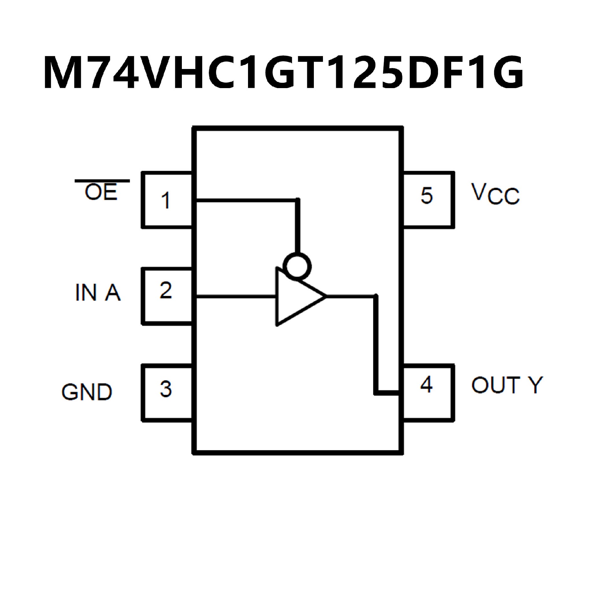


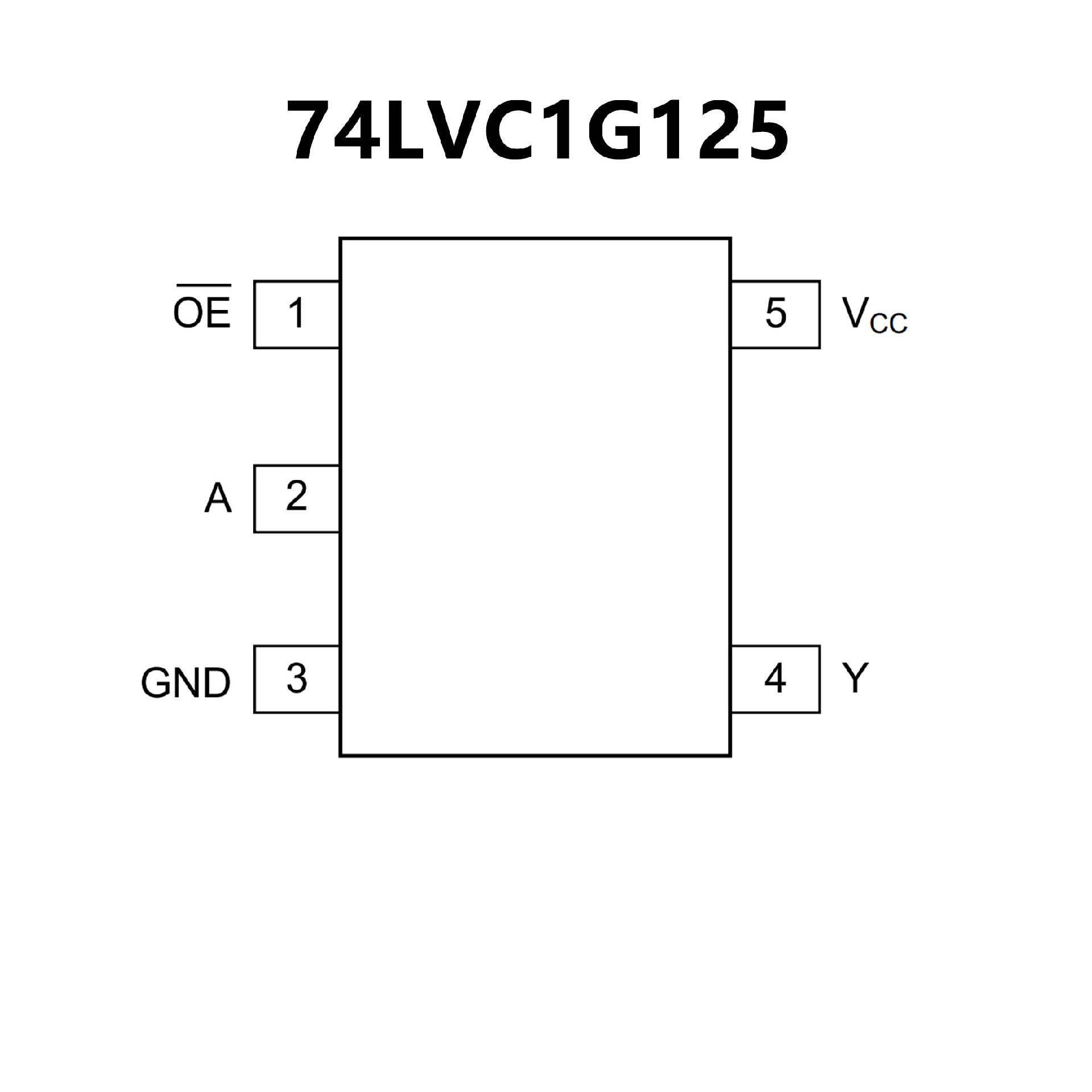
Bus Buffer/Line Driverwith 3-State Output,74LVC1G125 Replace M74VHC1GT125DF1G.
74LVC1G125 74LVC1G125.pdf
74LVC1G125.pdfFEATURES
• Wide Supply Voltage Range: 1.65V to 5.5V
• High Noise Immunity
• ±24mA Output Drive at VCC = 3.0V
• CMOS Low Power Consumption
• Inputs Accept Voltages Up to 5V
• Direct Interface with TTL Levels
• -40℃ to +125℃ Operating Temperature Range
• Available in a Green SC70-5 Package
PIN CONFIGUTION
CROSS
FEATURES
• High Speed: tPD = 3.5 ns (Typ) at VCC = 5 V
• Low Power Dissipation: ICC = 1µA (Max) at TA = 25°C
• TTL−Compatible Inputs: VIL = 0.8 V; VIH = 2 V
• CMOS−Compatible Outputs:
VOH > 0.8 VCC; VOL < 0.1 VCC @Load
• Power Down Protection Provided on Inputs and Outputs
• Balanced Propagation Delays
• Pin and Function Compatible
with Other Standard Logic Families
• Chip Complexity: FETs = 62; Equivalent Gates = 16
• Pb−Free Packages are Available
PIN CONFIGUTION