


High-speed USB 2.0 switch with enable, PI3USB221 Replace NX3DV221.
PI3USB221 PI3USB221.pdf
PI3USB221.pdfFEATURES
• VDD Operation at 2.5 V and 3.3 V
• VI/O Accepts Signals up to 5.5 V
• 1.8-V Compatible Control-Pin Inputs
• Low-Power Mode When OE Is Disabled (2 μA)
• rON = 6Ω Maximum
• ΔrON = 0.2Ω Typical
• Cio(on) = 6 pF Maximum
• Low Power Consumption (50 μA Maximum)
• ESD > 8kV contact on USB signal path per IEC61000-4-2)
• High Bandwidth (1.1 GHz Typical)
• Over Voltage Protection
• Packaging (Pb-free & Green): UQFN-10 and UDFN-10
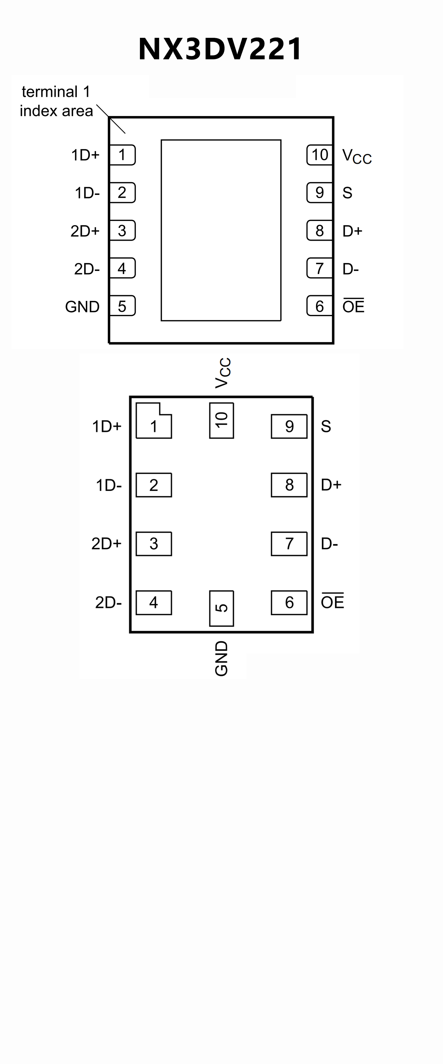
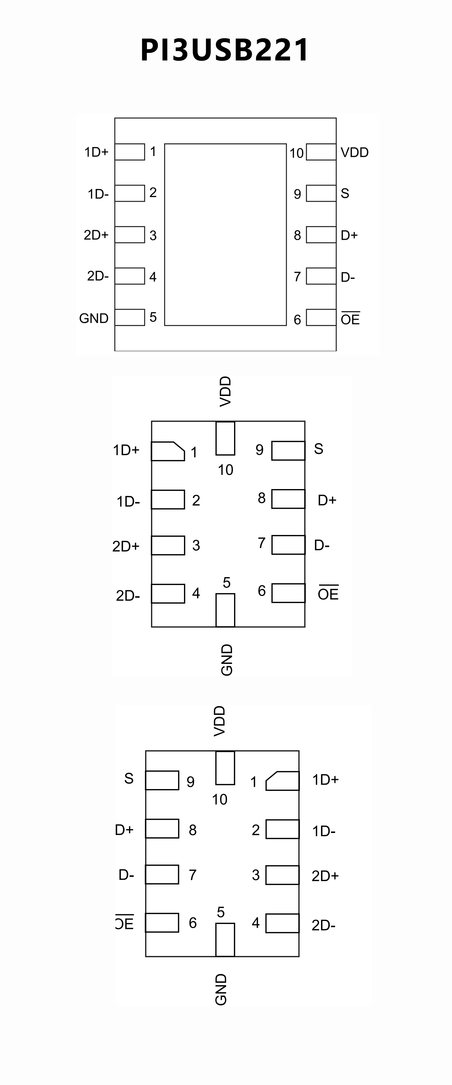
PIN CONFIGUTION
CROSS
FEATURES
• Wide supply voltage range from 2.3 V to 3.6 V
• Switch voltage accepts signals up to 5.5 V
• 1.8 V control logic at VCC = 3.6 V
• Low-power mode when OE is HIGH (2 A maximum)
• 6Ω(maximum) ON resistance
• 0.1Ω (typical) ON resistance mismatch between channels
• 6 pF (typical) ON-state capacitance
• High bandwidth (1.0 GHz typical)
• Latch-up performance exceeds 100 mA per JESD 78B Class
II Level A
• ESD protection:
• HBM JESD22-A114F Class 3A exceeds 8000 V
• CDM JESD22-C101E exceeds 1000 V
• HBM exceeds 12000 V for I/O to GND protection
• Specified from -40 ℃ to +85 ℃
PIN CONFIGUTION