


 PI6ULS5V9306QV8-7.pdf
• 2-bit Bidirectional Translator for SDA and SCL Lines in
Mixed-Mode I2C-Bus Applications
• Standard-Mode, Fast-Mode, and Fast-Mode Plus I2C-
Bus and SMBus Compatible
• Less than l.5ns Maximum Propagation Delay to
Accommodate Standard Mode and Fast Mode I2C-Bus
Devices and Multiple Masters
• Allows Voltage Level Translation Between:
◆ 0.9V VREF1 and 1.8V,2.5V,3.3V,or 5V VREF2
◆ 1.2V VREF1 and 1.8V,2.5V,3.3V,or 5V VREF2
◆ 1.5V VREF1 and 2.5V,3.3V,or 5V VREF2
◆ 1.8V VREF1 and 3.3V or 5V VREF2
◆ 2.5V VREF1 and 5V VREF2
◆ 3.3V VREF1 and 5V VREF2
• Provides Bidirectional Voltage Translation with no
Direction Pin
• Low 3.5O ON-State Connection Between Input and
Output Ports Provides Less Signal Distortion
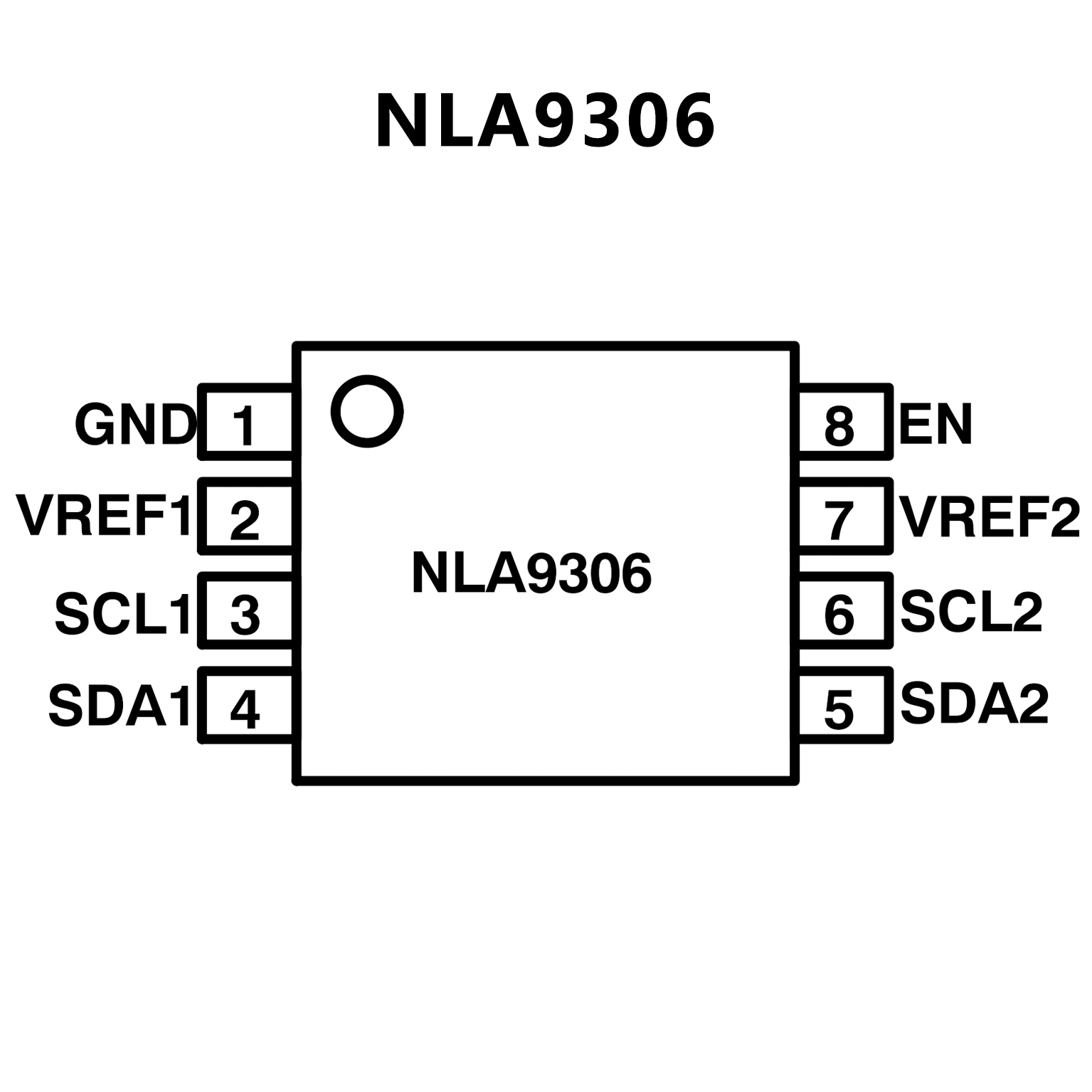
• Open-Drain I2C-Bus I/O Ports (SCLl, SDAl, SCL2,and
SDA2)
• 5V Tolerant I2C-Bus I/O Ports to Support Mixed-Mode
Signal Operation
• High-Impedance SCL1, SDAl, SCL2, and SDA2 Pins for
EN =LOW
• Lock-up Free Operation for Isolation when EN = LOW
• Flow through Pinout for Ease of Printed-Circuit Board
Trace Routing
• ESD Protection Exceeds 4KV HBM per JESD22-Al14
• Totally Lead-Free & Fully RoHS Compliant (Notes 1 & 2)
• Halogen and Antimony Free. “Green" Device (Note 3)
• The PI6ULS5V9306Q is suitable for automotive applications
requiring specific change control; this part is AEC-Q100
qualified, PPAP capable, and manufactured in IATF 16949
certified facilities.
• Packaging (Pb-free & Green): 8-Pin,VSSOP (V)
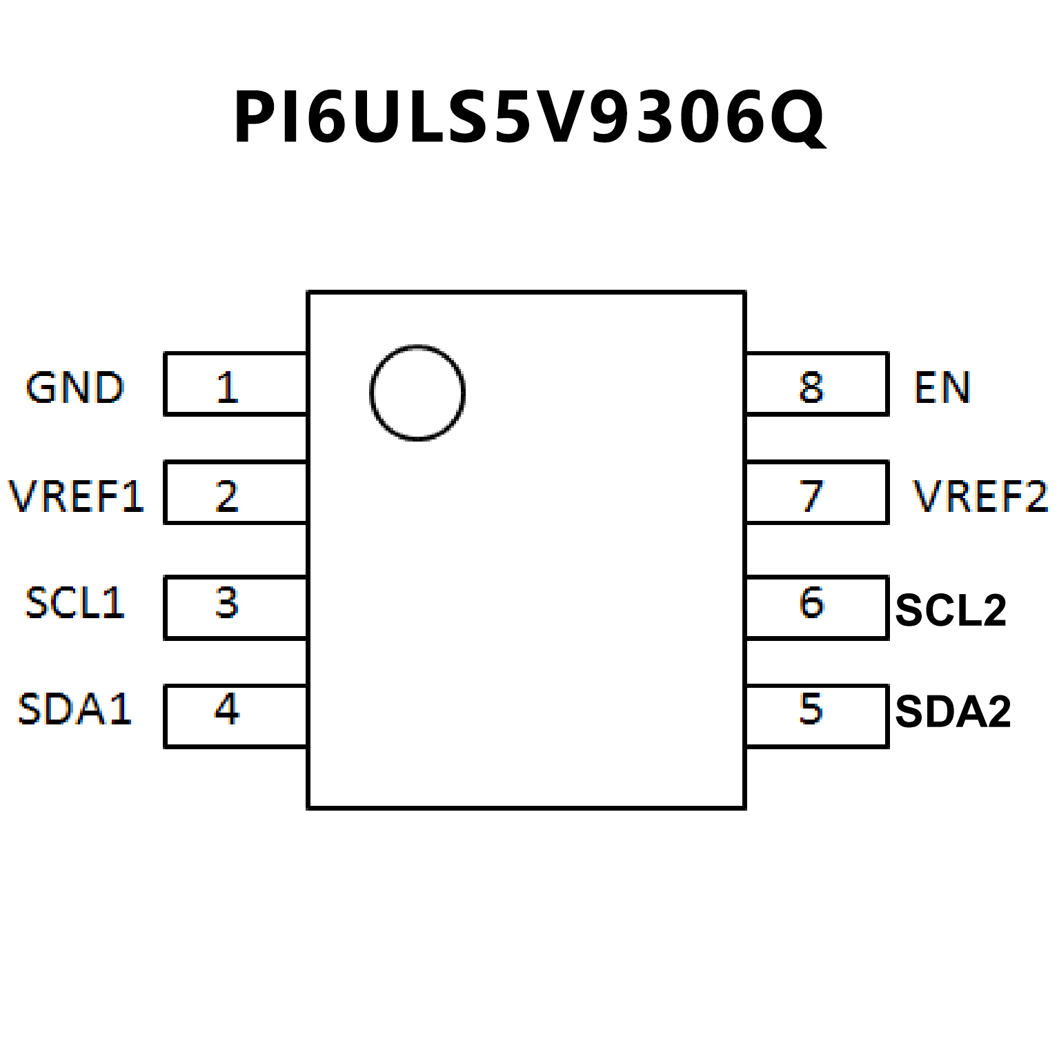
• 2−bit Bidirectional Translator for SDA and SCL Lines in
• Open−Drain I2C−Bus I/O Ports (SCL1, SDA1, SCL2
and SDA2)
are RoHS Compliant