


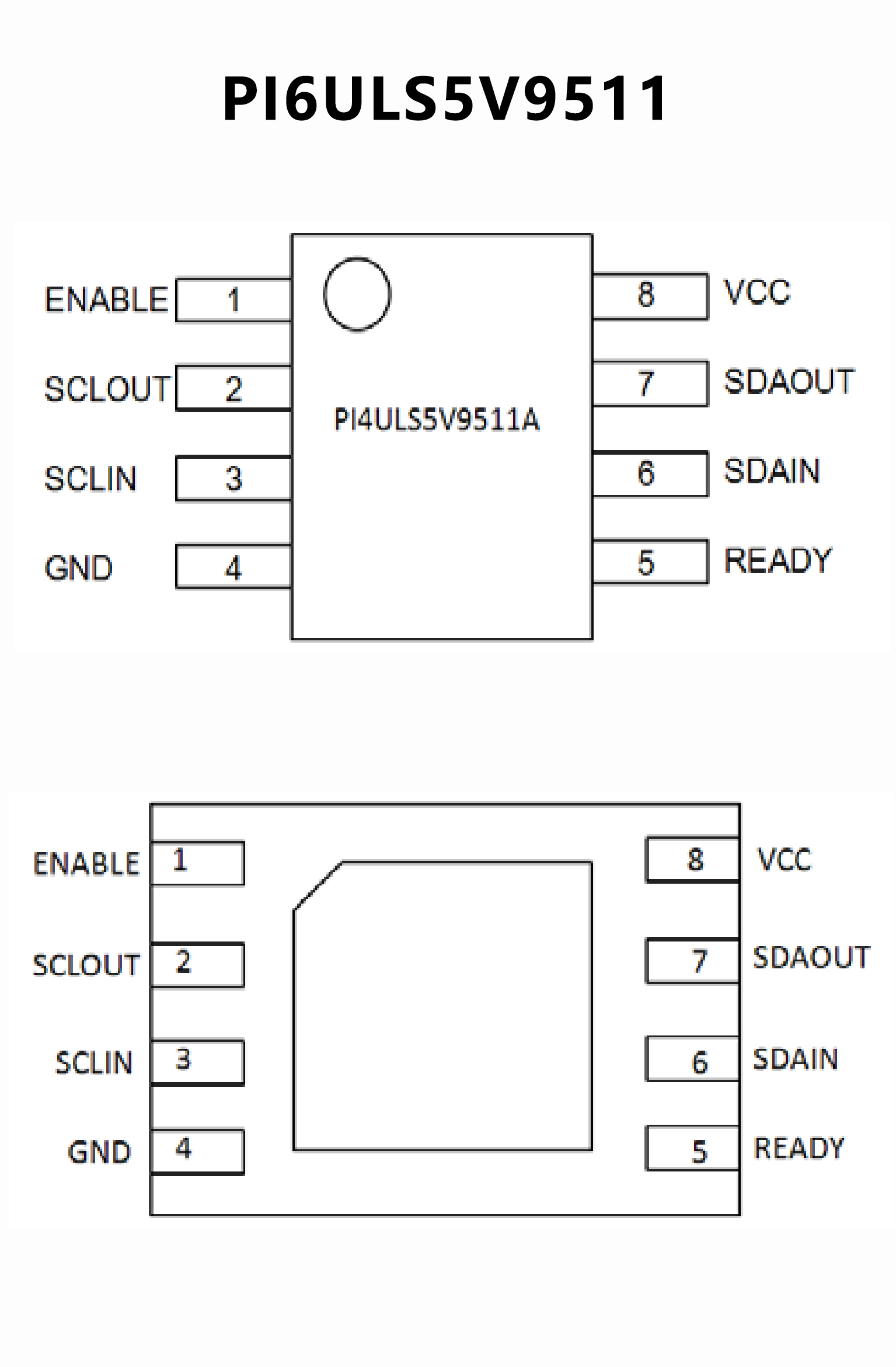
Hot swappable I2C-bus and SMBus bus buffer, PI6ULS5V9511 Replace PCA9511.
PI6ULS5V9511 PI6ULS5V9511.pdf
PI6ULS5V9511.pdfFEATURES
• Bidirectional Buffer for SDA and SCL Lines Increases
Fan Out
• Prevents SDA and SCL Corruption During Live Board
Insertion and Removal from Backplane
• Isolates Input SDA and SCL Lines From Output
• Compatible with I2C, I2C Fast Mode, and SMBus
Standards (up to 400kHz Operation)
• Built-in Rise-Time Accelerators on all SDA and SCL
• Wide Supply Voltage Range: 2.7V to 5.5V
• Active HIGH ENABLE Input
• Active HIGH READY Open-Drain Output
• High-Impedance SDA and SCL pins for VCC = 0V
• 1.1V Pre-Charge on all SDA and SCL Lines
• Supporting Clock Stretching and Multiple Master
Arbitration/Synchronization
• ESD Protection Exceeds 4000V HBM per JESD22-A114
• Packages Offered: MSOP-8(U), UDFN-8(ZW), and
SOIC-8(W)
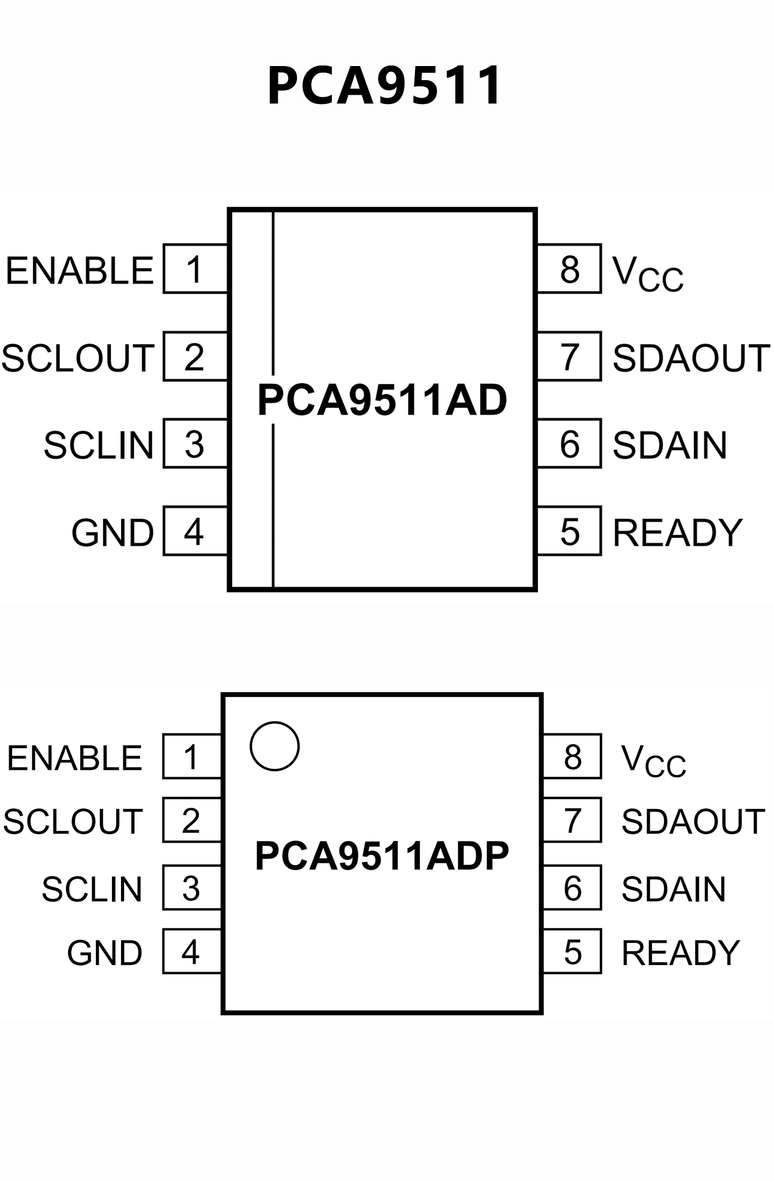
PIN CONFIGUTION
CROSS
FEATURES
• Bidirectional buffer for SDA and SCL lines increases fan out
and prevents SDA and SCL corruption during live board
insertion and removal from multipoint backplane systems
• Compatible with I2C-bus Standard-mode, I2C-bus Fast-
mode, and SMBus standards
• Built-in ∆V/∆t rise time accelerators on all SDA and SCL
lines (0.6 V threshold) requires the bus pull-up voltage and
supply voltage (VCC) to be the same
• Active HIGH ENABLE input
• Active HIGH READY open-drain output
• High-impedance SDA and SCL pins for VCC =0V
• 1 V precharge on all SDA and SCL lines
• Supporting clock stretching and multiple master arbitration/
synchronization
• Operating power supply voltage range: 2.7 V to 5.5 V
• 0 Hz to 400 kHz clock frequency
• ESD protection exceeds 2000 V HBM per JESD22-A114,
200 V MM per
JESD22-A115, and 1000 V CDM per JESD22-C101
• Latch-up testing is done to JEDEC Standard JESD78 which
exceeds 100 mA
• Packages offered: SO8, TSSOP8 (MSOP8)
PIN CONFIGUTION