


 SGM48017.pdf
• Simple and Reliable
• 6.4A Source and 7.6A Sink Peak Currents
• Operate in 4.5V to 20V Supply Range
• Fast Propagation Delays: 30ns (TYP)
• Fast Rise Time: 11ns (TYP)
• Fast Fall Time: 11ns (TYP)
• Ringing Suppression
• Recovery Time of UVLO Less than 2μs
• Ability to IN Handle Negative Voltages: -10V
(VDD - VIN_MIN ≤ 22V)
• Ability to OUT Handle Negative Voltages: -5V
(500ns)
• Comprehensive Protection Features Over-Voltage
Protection Under-Voltage Lockout Short-Circuit
Protection
• -40℃ to +125℃ Operating Temperature Range
• Available in a Green SOT-23-5 Package

• Low-Cost Gate-Driver Device
Offering Superior Replacement of NPN
and PNP Discrete Solutions
• 4-A Peak Source and 8-A Peak Sink Asymmetrical Drive
• Strong Sink Current Offers Enhanced Immunity
Against Miller Turnon
• Split Output Configuration
(Allows Easy and Independent
Adjustment of Turnon and Turnoff Speeds)
in the UCC27511 Saves 1 Diode
• Fast Propagation Delays (13-ns Typical)
• Fast Rise and Fall Times (9-ns and 7-ns Typical)
• 4.5-V to 18-V Single Supply Range
• Outputs Held Low During VDD UVLO (Ensures
Glitch-Free Operation at Power Up and Power Down)
TTL and CMOS Compatible Input-Logic Threshold
(Independent of Supply Voltage)
• Hysteretic-Logic Thresholds for High-Noise Immunity
• Dual-Input Design (Choice of an Inverting (IN–Pin)
or Noninverting (IN+ Pin) Driver Configuration)
Unused Input Pin can be
Used for Enable or Disable Function
• Output Held Low When Input Pins Are Floating
• Input Pin Absolute Maximum Voltage Levels Not
Restricted by VDD Pin Bias Supply Voltage
Operating Temperature Range of –40°C to 140°C
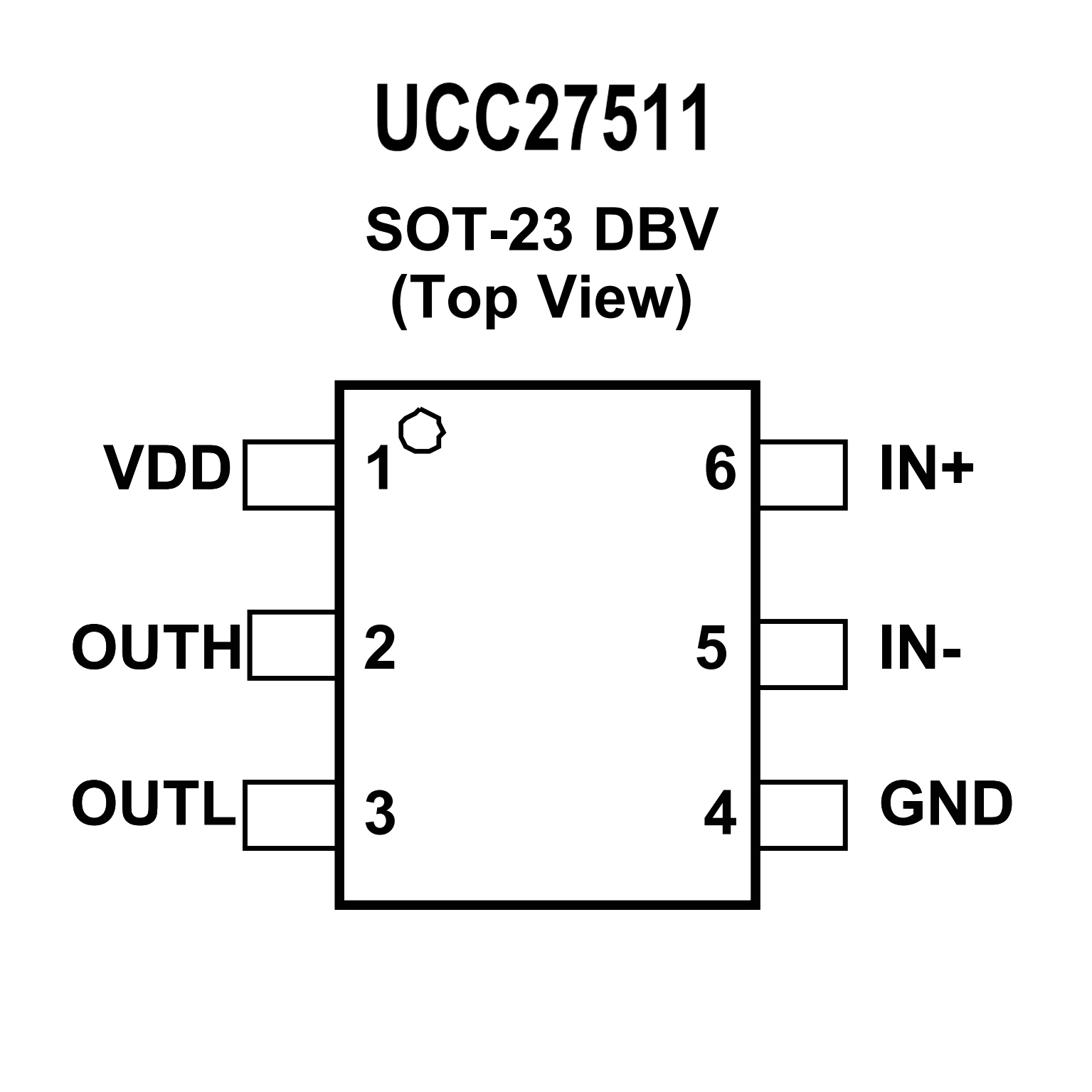
• 6-Pin DBV (SOT-23) and 6-Pin DRS (3-mm ×
3-mm WSON With Exposed Thermal Pad) Package Options