


 SGM48523.pdf
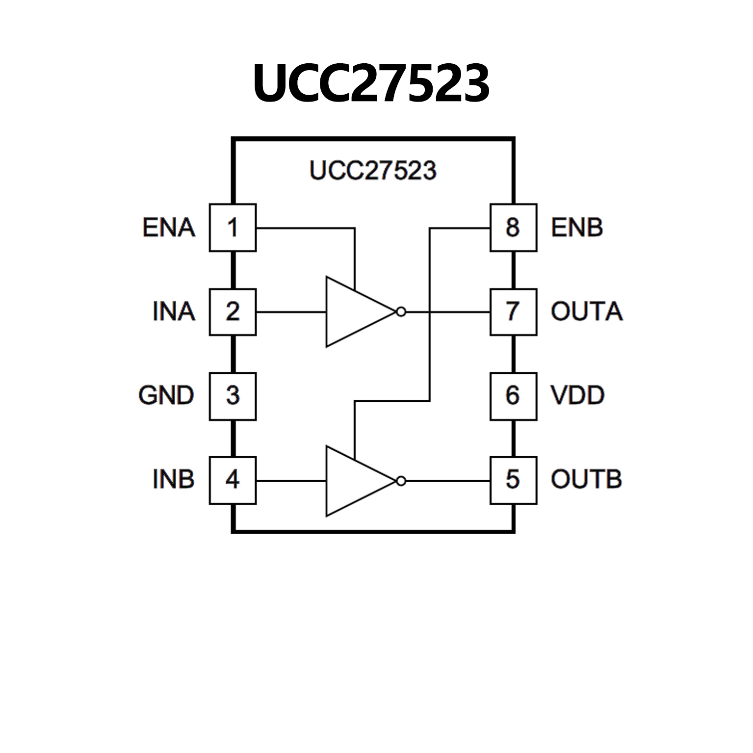
• Two Independent Gate Drive Channels
• 4.5V to 18V Single Supply Range (VDD)
• 5A Peak Source/Sink Pulse Current Drive
• Independent Enable Pin for Each Channel
• TTL and CMOS Compatible Logic Threshold
• Logic Levels Independent of Supply Voltage
• Hysteretic Input Logic for High Noise Immunity
• Outputs are Logic Low when Inputs are Floating
• Negative Voltage Handling Capability:-8V DC at
Inputs-2V, 200ns Pulse for Outputs (OUTx)
• Glitch-Free Operation at Power-Up and Power-
Down: Outputs Pulled Low during Supply UVLO
• Fast Propagation Delays: 18ns (TYP)
• Fast Rise Time: 8ns (TYP)
• Fast Fall Time: 8ns (TYP)
• Delay Matching between Two Channels: 1ns (TYP)
• Channels can be Paralleled for Higher Drive Current
• -40℃ to +140℃ Operating Temperature Range
• Available in Green SOIC-8, MSOP-8 (Exposed Pad)
and TDFN-3×3-8L Packages

• Industry-Standard Pinout
• Two Independent Gate-Drive Channels
• 5-A Peak Source and Sink-Drive Current
• Independent-Enable Function for Each Output
• TTL and CMOS Compatible Logic Threshold
• Independent of Supply Voltage
• Hysteretic-Logic Thresholds for High Noise Immunity
• Inputs and Enable Pin-Voltage Levels
Not Restricted by VDD Pin Bias Supply Voltage
• 4.5-V to 18-V Single-Supply Range
• Outputs Held Low During VDD-UVLO, (Ensures
Glitch-Free Operation at Power up and Power Down)
• Fast Propagation Delays (13-ns Typical)
• Fast Rise and Fall Times (7-ns and 6-ns Typical)
• 1-ns Typical Delay Matching Between Two Channels
• Two Outputs are in Parallel for Higher Drive Current
• Outputs Held Low When Inputs Floating
• PDIP (8), SOIC (8), MSOP (8) PowerPAD™ and
• 3-mm × 3-mm WSON-8 Package Options
• Operating Temperature Range of –40°C to 140°C