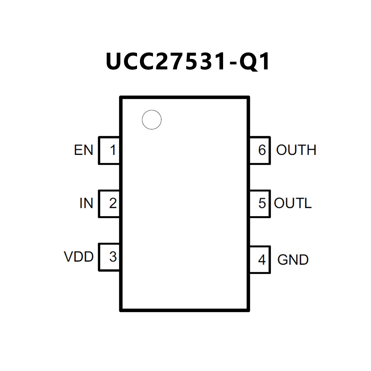
• Qualified for Automotive Applications
• AEC-Q100 Qualified with the Following Results:
Device Temperature Grade 1
Device HBM ESD Classification Level H2
Device CDM ESD Classification Level C4B
• Low Cost Gate Driver (Offering Optimal
Solution for Driving Fet And Igbts)
• Superior Replacement to Discrete Transistor Pair
Drive (Providing Easy Interface With Controller)
TTL and CMOS Compatible Input Logic
Threshold, (Independent of Supply Voltage)
• Split Output Options Allow for
Tuning of Turn-On and Turn-Off Currents
• Enable with Fixed TTL Compatible Threshold
• High 2.5-A Source and 5-A Sink
Peak Drive Currents at 18-V VDD
• Wide VDD Range From 10 V up to 35 V
• Input and Enable Pins Capable of
Withstanding up to –5-V DC Below Ground
• Output Held Low When Inputs are
Floating or During VDD UVLO
• Fast Propagation Delays (17-ns Typical)
• Fast Rise and Fall Times
(15-ns and 7-ns Typical With 1800-pF Load)
• Undervoltage Lockout (UVLO)
• Used as a High-Side or Low-Side Driver
(if Designed With Proper Bias and Signal Isolation)
Low-Cost, Space-Saving
6-Pin DBV (SOT-23) Package Options
• Operating Temperature Range of –40°C to 140°C


 SGM48536Q.pdf

