


Low- and High-Side Voltage Output, Current-Sense Amplifiers, ZXCT180 Replace INA180.
ZXCT180 ZXCT180.pdf
ZXCT180.pdfFEATURES
• Supply Voltage Range: 2.7V to 5.5V
• Wide Common-Mode Range: -0.3V to 26V
• Gain Error: (Maximum over Temperature): ±1%
• Choice of Gains:
▪ Pinout A1 and B1: 20V/V
▪ Pinout A2 and B2: 50V/V
▪ Pinout A3 and B3: 100V/V
▪ Pinout A4 and B4: 200V/V
• Low Offset Voltage: Typical ±100μV and 1-µV/°C Drift
• Rail-to-Rail Output Capability
• Low Quiescent Current: 370μA (max)
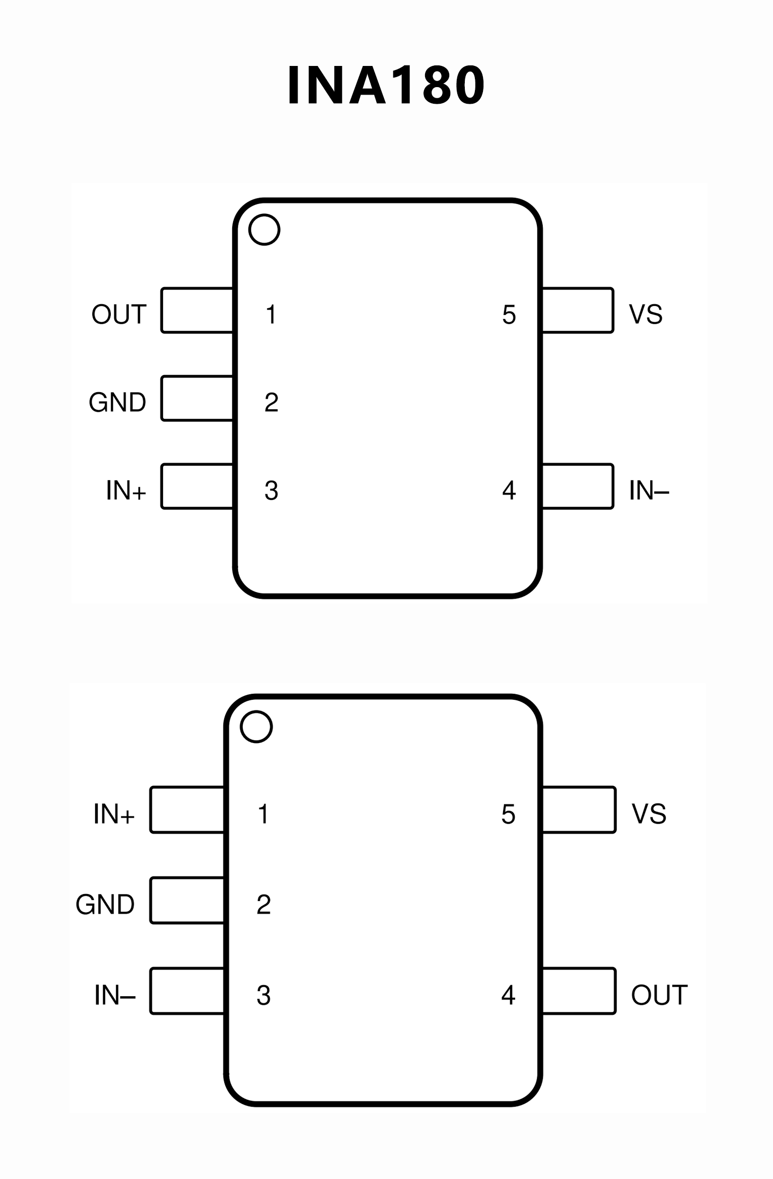
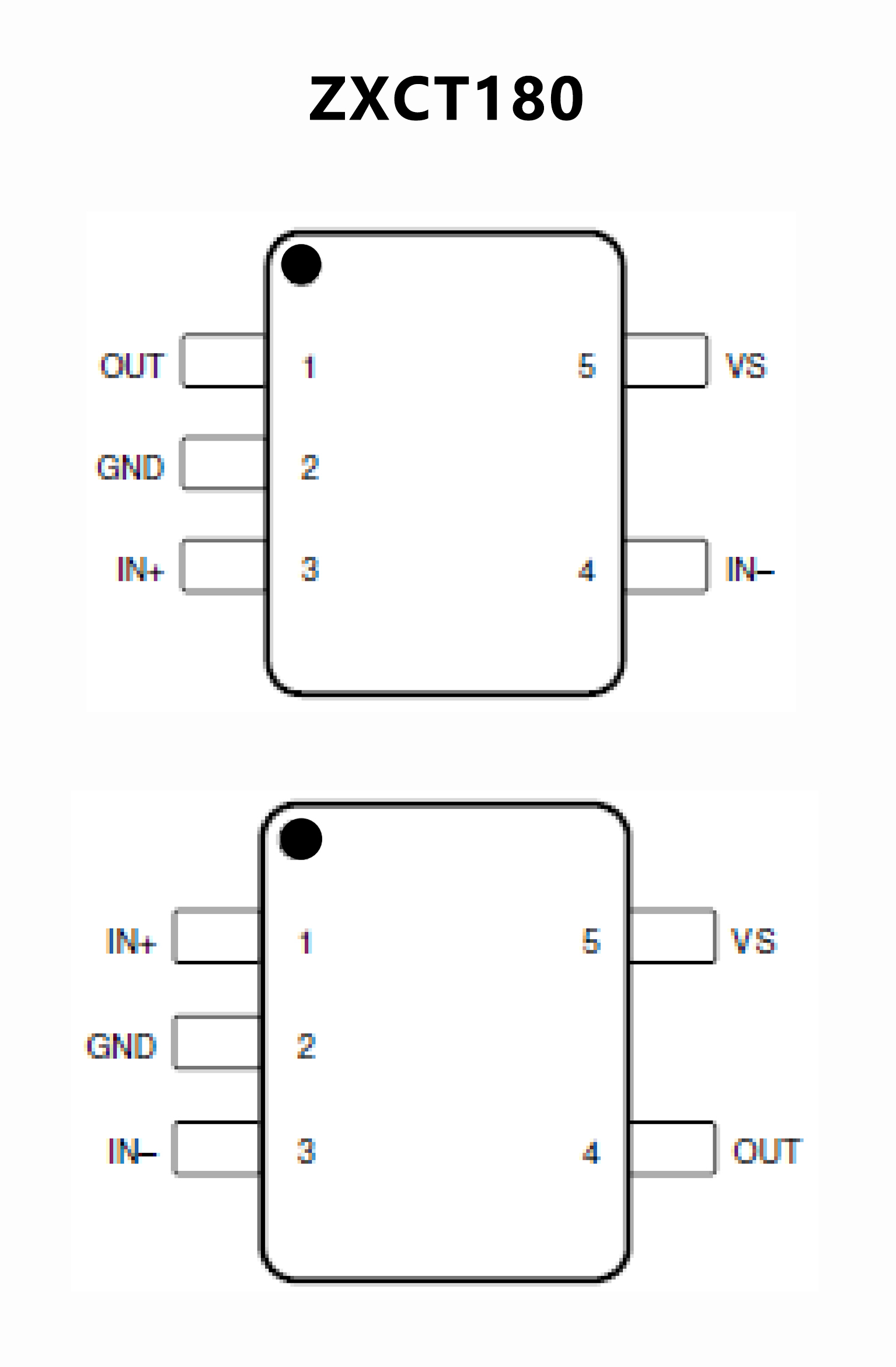
• Package: 5-Pin SOT25
• ESD Protection JESD 22, 5000V HBM (A114)
• Totally Lead-Free & Fully RoHS Compliant (Notes 1 & 2)
• Halogen and Antimony Free. “Green” Device (Note 3)
• For automotive applications requiring specific change
control
PIN CONFIGUTION
CROSS
FEATURES
• Common-mode range (VCM): –0.2 V to +26 V
• High bandwidth: 350 kHz (A1 devices)
• Offset voltage:
– ±150 µV (maximum) at VCM = 0 V
– ±500 µV (maximum) at VCM = 12 V
• Output slew rate: 2 V/µs
• Accuracy:
– ±1% gain error (maximum)
– 1-µV/°C offset drift (maximum)
• Gain options:
– 20 V/V (A1 devices)
– 50 V/V (A2 devices)
– 100 V/V (A3 devices)
– 200 V/V (A4 devices)
• Quiescent current: 260 µA maximum (INA180)
PIN CONFIGUTION