


 74LVC1G07SE-7.pdf
No.10519
• Wide Supply Voltage Range from 1.65 to 5.5V
• ± 24mA Output Drive at 3.3V
• CMOS Low Power Consumption
• IOFF Supports Partial-Power-Down Mode Operation
• Inputs Accept Up to 5.5V
• Latch-Up Exceeds 100mA per JESD 78, Class I
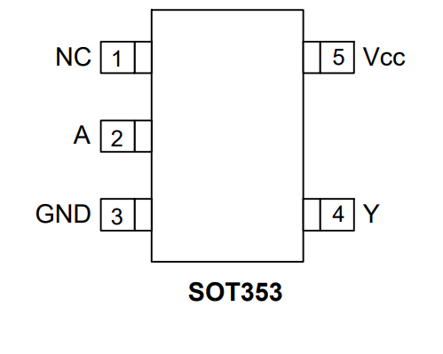
• Range of Package Options
• Direct Interface with TTL Levels
The 74LVC1G07 is a single buffer gate with an open-drain output. The device is designed for operation with a power supply range of 1.65V to 5.5V. The input is tolerant to 5.5V allowing this device to be used in a mixed voltage environment. The device is fully specified for partial power down applications using IOFF. The IOFF circuitry disables the output preventing damaging current backflow when the device is powered down. The open-drain output can be connected to other open drain outputs to implement active-low wired-OR or active-high wired-AND functions. The maximum sink current is 32mA.