


 SGM48523.pdf
No.11694
• Two Independent Gate Drive Channels
• 4.5V to 18V Single Supply Range (VDD)
• 5A Peak Source/Sink Pulse Current Drive
• Independent Enable Pin for Each Channel
• TTL and CMOS Compatible Logic Threshold
• Logic Levels Independent of Supply Voltage
• Hysteretic Input Logic for High Noise Immunity
• Outputs are Logic Low when Inputs are Floating
• Negative Voltage Handling Capability:
-8V DC at Inputs
-2V, 200ns Pulse for Outputs (OUTx)
• Glitch-Free Operation at Power-Up and Power
Down: Outputs Pulled Low during Supply UVLO
• Fast Propagation Delays: 18ns (TYP)
• Fast Rise Time: 8ns (TYP)
• Fast Fall Time: 8ns (TYP)
• Delay Matching between Two Channels: 1ns (TYP)
• Channels can be Paralleled for Higher Drive Current
• -40℃ to +140℃ Operating Temperature Range
• Packaging:
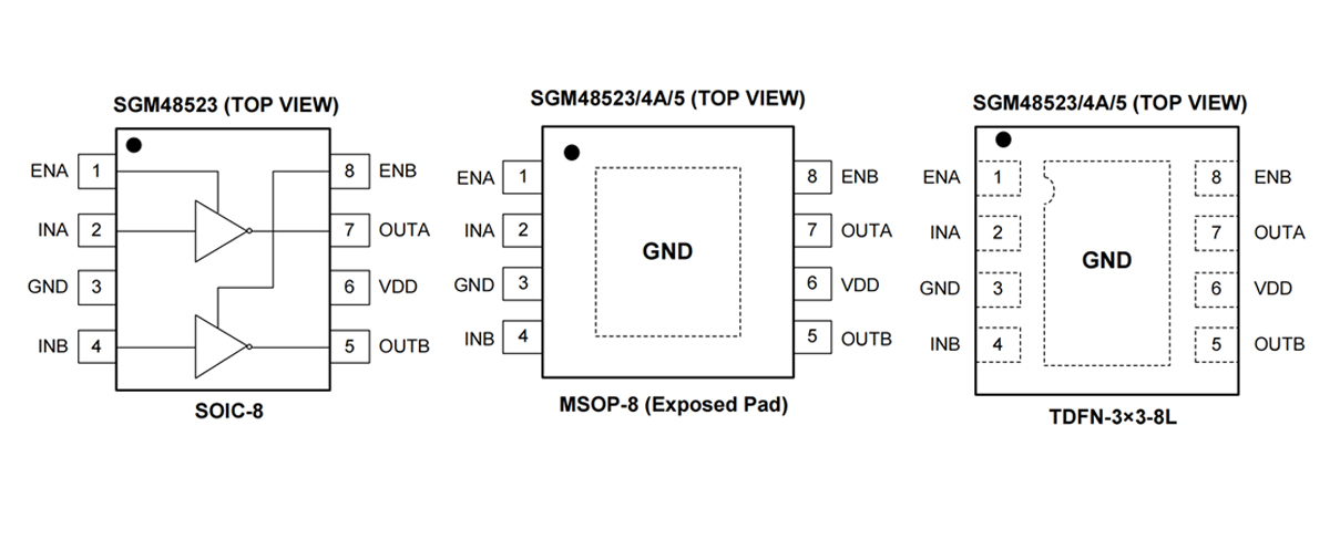
SGM48523/4A/5 Available in Green SOIC-8, MSOP-8
(Exposed Pad) and TDFN-3×3-8L Packages
SGM48526 Available in a Green TDFN-3×3-8L
Package
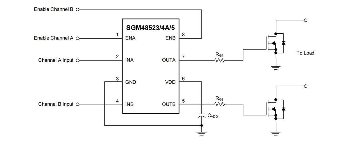
The SGM48523/4A/5/6 are dual high-speed low-side gate drivers for MOSFET and IGBT power switches. They have rail-to-rail driving capability and can sink and source up to 5A peak current with capacitive loads. The propagation delays are very short and well matched between the two channels that make the device very fit for applications that need accurate dual gate driving such as synchronous rectifiers. The matched propagation delays also allow for paralleling the two channels when higher driving current is required for example for paralleled switches. The input voltage thresholds are fixed, independent of supply voltage (VDD) and are compatible with low voltage TTL and CMOS logic. Noise immunity is excellent due to the wide hysteresis window between the input low and high thresholds. The devices have internal pull-up/pull-down resistors on the input pins to ensure low state on the driver outputs when the inputs are floating.
The SGM48523/4A/5 offer 3 logic options: dual inverting (SGM48523), dual non-inverting (SGM48524A), and one inverting and one non-inverting (SGM48525). They have independent enable pins (ENA and ENB) for each channel with active-high logic that can be left open for normal operation because of internal pull-up to VDD.The SGM48526 offers a flexible dual input design which can be configured as inverting (-INx) or non-inverting (+INx) for each channel. Both inputs (+INx or -INx) can control the output state. Typically, one input is used for gate pulse and the other one is used for enable/disable function.
The SGM48523/4A/5 are available in SOIC-8, MSOP-8 (Exposed Pad) and TDFN-3×3-8L packages. The SGM48526 is available in a Green TDFN-3×3-8L package. They operate over a temperature range of -40℃ to +140℃.