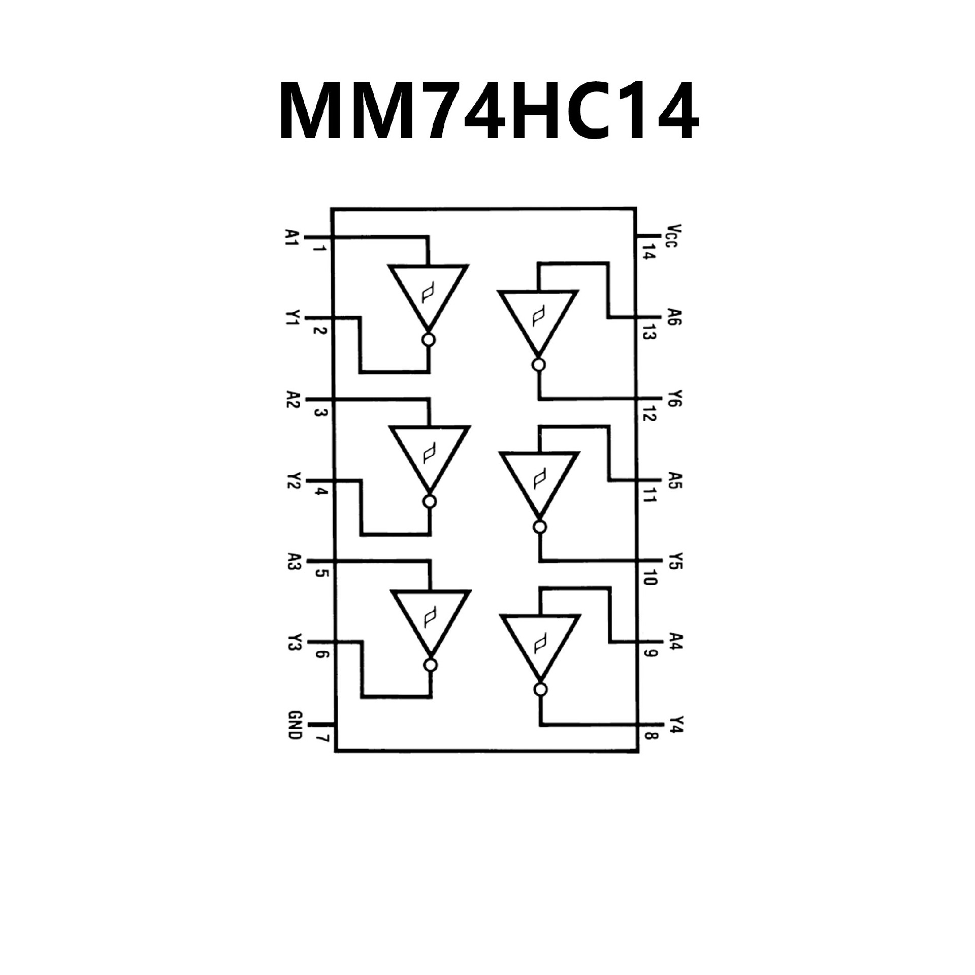


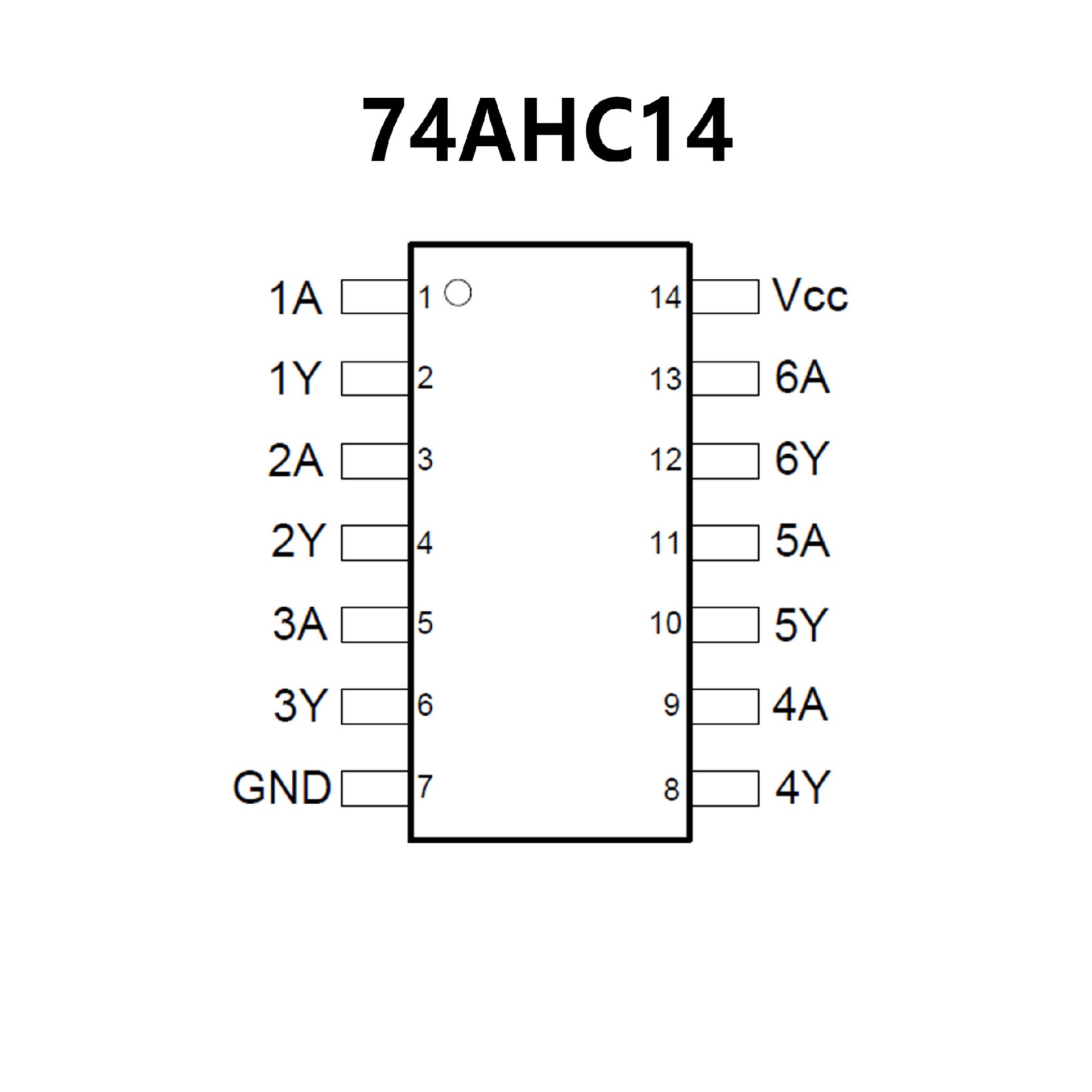
 74AHC14.pdf
• Wide Supply Voltage Range from 2.0V to 5.5 V
• Outputs Sink or Source 8mA at VCC = 4.5V
• CMOS Low Power Consumption
• Schmitt Trigger Action at All Inputs
• Typical hysteresis of 1V allows for
transformation of slow
changing input signals to sharply
defined, fast transition output signals.
• Inputs can be driven by 3.3V or
5.5V allowing for voltage
translation applications.
• ESD Protection Exceeds JESD 22
200-V Machine Model (A115-A)
2000-V Human Body Model (A114-A)
Exceeds 1000-V Charged Device Model (C101C)
• Latch-Up Exceeds 250mA per JESD 78, Class II
• Range of Package Options SO-14 and TSSOP-14
• Totally Lead-Free & Fully
RoHS Compliant (Notes 1 & 2)
• Halogen and Antimony Free.
“Green” Device (Note 3)
• Typical propagation delay: 13ns
• Wide power supply range: 2V–6V
• Low quiescent current: 20μA maximum (74HC Series)
• Low input current: 1μA maximum
• Fanout of 10 LS-TTL loads
• Typical hysteresis voltage: 0.9V at VCC = 4.5V