 SGM4551.pdf
• 2-Bit Bidirectional Translator for
SDA and SCL Lines in Mixed-
Mode I2C Applications
• I2C and SMBus Compatible
• Less than 5.5ns Propagation Delay to
Accommodate Standard-Mode and
Fast-Mode I2C Devices and Multiple Masters
• Allows Voltage-Level Translator Between
1.2V VREF1 and 1.8V, 2.5V, 3.3V, or 5V VREF2
1.8V VREF1 and 2.5V, 3.3V, or 5V VREF2
2.5V VREF1 and 3.3V or 5V VREF2
3.3V VREF1 and 5V VREF2
• Provides Bidirectional Voltage
Translation with No Direction Pin
• Low 3.5Ω ON-State Connection Between
Input and Output Ports
Provides Less Signal Distortion
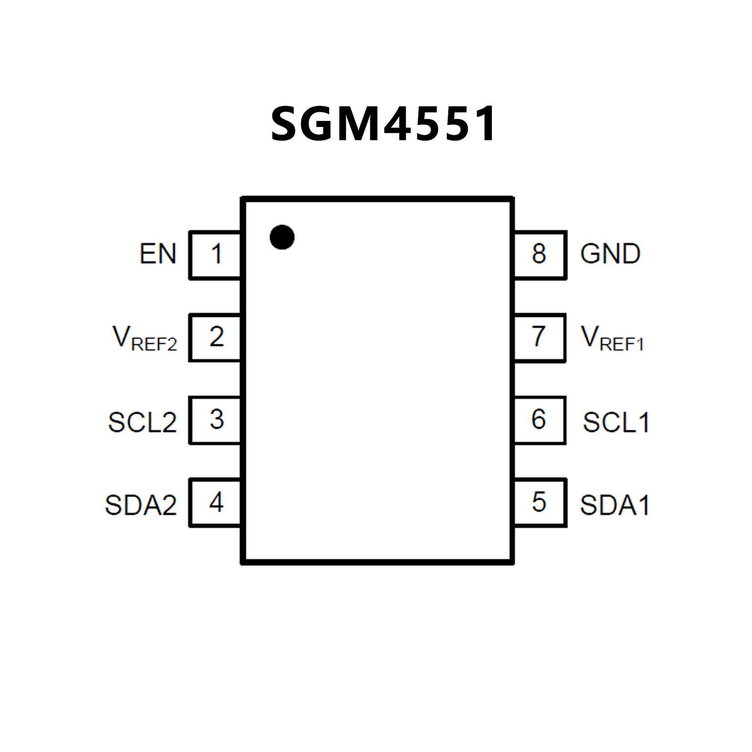
• Open-Drain I2C I/O Ports
(SCL1, SDA1, SCL2, and SDA2)
• 5V Tolerant I2C I/O Ports to Support
Mixed-Mode Signal Operation
• High-Impedance SCL1, SDA1, SCL2, and
SDA2 Pins for EN = Low
• Lock-Up-Free Operation for Isolation When EN = Low
• Flow-Through Pinout for Ease of Printed
Circuit Board Trace Routing
• Available in Green SOT-23-8 and
XTDFN-1.4×1-8L Packages
• Available in the Texas Instruments
NanoFree™ Packages
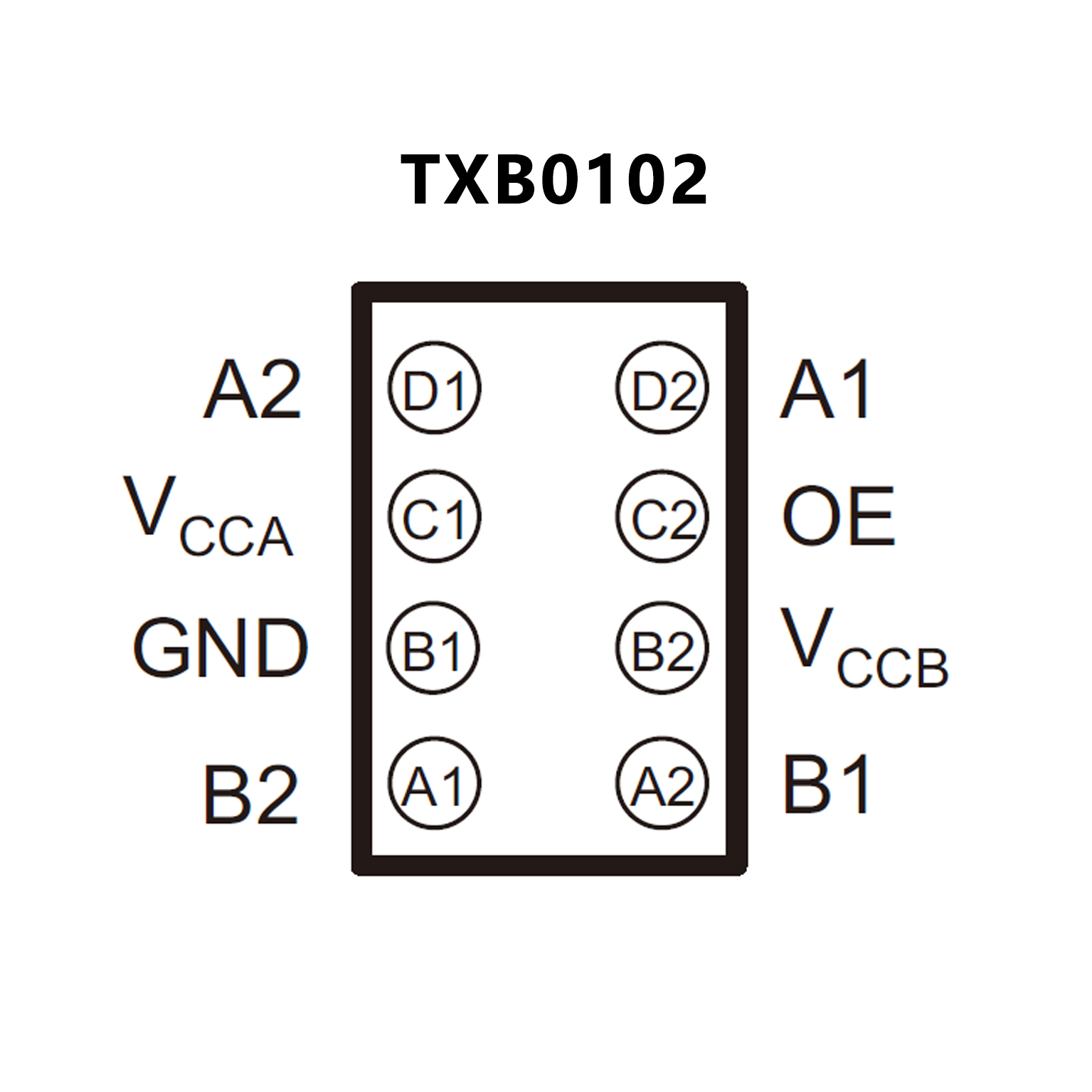
• 1.2 V to 3.6 V on A Port and 1.65 V to
5.5 V On B Port (VCCA ≤ VCCB)
• VCC Isolation Feature – If Either VCC
Input Is at GND, All Outputs Are in
the High-Impedance State
• OE Input Circuit Referenced to VCCA
• Low Power Consumption, 4-µA Max ICC
• Ioff Supports Partial-Power-
Down Mode Operation
• Latch-Up Performance Exceeds 100
mA Per JESD 78, Class II
• ESD Protection Exceeds JESD 22
A Port2500-V Human-Body Model (A114-B)
200-V Machine Model (A115-A)
1500-V Charged-Device Model (C101)
B Port15-kV Human-Body Model (A114-B)
200-V Machine Model (A115-A)
1500-V Charged-Device Model (C101)
